Enhanced crystallinity of the perovskite semiconductor films doped with MBI molecule
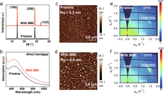
The phase purity of recrystallized MBI was investigated by X-ray diffraction (XRD) (Fig. S1)21. The XRD results presented in Fig. 1a and Supplementary Fig. 2 indicate that the crystallinity of the perovskite films was enhanced following MBI doping. Fullwidth at half-maximum (FWHM) and peak position of (110) crystal plane in XRD of perovskite films with different MBI concentrations are provided in Supplementary Tables 1, 2. Compared with pristine, the FWHW of MBI-doped perovskite film decreases on (100), denoting crystallinity has been improved. All perovskite films exhibit three dominant peaks at around 14°, 28°, and 33°, corresponding to the (100), (200), and (122) crystal planes of the FASnI315. The doping of the MBI molecules enhances the absorption ability, while the absorption peak position remains unchanged, indicating that the introduction of MBI does not change the body structure (Fig. 1b). MBI was not incorporated into the crystal lattice. The primary material employed was a 2D/3D perovskite composite, with the 2D component constituting 6.7 mol% of the overall material. XRD analysis revealed the characteristic crystal plane peaks associated with the 3D perovskite structure. The enhancement in absorption coefficient and the improved crystallinity demonstrates a significant improvement in the quality of the film following the introduction of MBI molecules. The rise in crystallinity further indicates a more orderly arrangement of the perovskite spatial structure. Analysis of the AFM images reveals that both films exhibit low roughness (Rq). Furthermore, the average grain size of the film incorporating 0.5 mol% MBI molecules is larger compared to the pristine films (Fig. 1c, d). After introducing MBI molecules, the crystallinity of grains increased, mainly reflected in the increase of grain size and longitudinal growth from the SEM images (Supplementary Fig. 3). We used grazing-incidence wide-angle X-ray scattering (GIWAXS) to scrutinize the orientation of the crystal structure further. As illustrated in Fig. 1e, f, while the pristine perovskite film displays broad Debye-Scherrer rings indicative of random orientation within the perovskite grains, the perovskite film doped with 0.5 mol% MBI exhibits distinct Bragg points, signifying a high degree of crystal orientation. The other GIWAXS results with various doping concentrations are presented in Supplementary Fig. 4, suggesting improved crystallinity after the introduction of MBI molecular. The time-resolved photoluminescence (TRPL) results reveal an increase in the average carrier lifetime of perovskite films with MBI, further underscoring the enhancement in film quality (Supplementary Fig. 5). This orderly arrangement lays the foundation for the emergence of ferroelectricity. Moreover, the improved film quality mitigates the defect-induced shielding effect on the ferroelectricity.

a XRD pattern, b absorption spectra (film thickness = 38 nm), c, e are the AFM and GIWAXS data for the pristine films. d, f are the AFM and GIWAXS data for the films doped with the MBI molecule.
Ferroelectricity validation of reconfigured perovskite semiconductors
Next, piezoelectric atomic force microscope (PFM) and switching spectroscopy PFM (SS-PFM) were used to discover evidence of ferroelectricity in the perovskite semiconductors incorporated with the MBI molecule. The thickness of all perovskite films is about 38 nm. As depicted in Fig. 2a, b, the PFM out-of-plane (OOP) phase and amplitude images of the pristine film did not exhibit a signal driven by alternating current (AC) bias. The local phase and amplitude curves of the pristine perovskite film are shown in Fig. 2c, which do not exhibit any ferroelectric characteristics. On the contrary, the OOP phase and amplitude image of perovskite films doped with 0.5 mol% MBI molecule exhibit distinct contrast, dedicating existing piezoelectric response. The OOP phase image reveals a distinctly clear boundary, while the OOP amplitude image exhibits amplitude variations exceeding 12 pm (Fig. 2d, e), which demonstrates that the film undergoes a 180-degree domain flip when driven by AC bias and exhibits contraction or expansion when driven by voltage. The well-defined hysteresis loops and “butterfly” curves compellingly demonstrate the robust ferroelectricity in doped 0.5 mol% MBI molecule perovskite films (Fig. 2f). The other PFM and SS-PFM results with various doping concentrations are presented in the Supplementary Fig. 6 and Fig. 7, suggesting again that the doping of MBI molecule can bring the ferroelectricity for perovskite semiconductors.
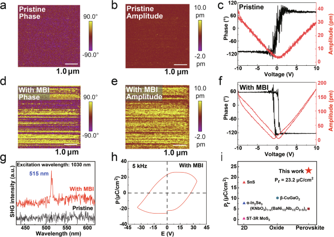
a, b are the PFM phase and amplitude for the pristine films. d and e are the PFM phase and amplitude for the films doped with MBI molecule. c, f are SS-PFM data for the pristine and the doped films, g SHG spectra of the pristine and doped films. h Polarization-electric-field loops measured with a metal-insulator-semiconductor-metal capacitor for doped films. i Our Pr value compared to the other ferroelectric semiconductors. Piezoelectric hysteresis loops of PFM were conducted by applying direct current (DC) bias that sweeps from −10.0 to 10.0 V.
Second harmonic generation (SHG) spectroscopy is an efficient technique to ascertain spatial symmetry breaking. Compared to the pristine film, the perovskite film doped with 0.5 mol% MBI molecule exhibits an obvious frequency-doubled signal at 515 nm (Fig. 2g), confirming the spatial symmetry breaking. As we know, the remnant polarization intensity (Pr) is key parameters used to evaluate the ferroelectric properties of materials. However, obtaining parameters in ferroelectric semiconductors is challenging, as the leakage current in these materials can obscure the polarization switching current. To determine these values and further confirm the presence of ferroelectricity, a ferroelectric analyzer was employed to test the pristine and with MBI films, using metal-insulator-semiconductor-metal (MISM) structure to decrease leakage current. The polarization–electric field (P-E) hysteresis loop is shown in Fig. 2h, we can find a typical rectangular P-E ferroelectric loop, indicating obvious ferroelectric characteristics. The material is a ferroelectric semiconductor, which differs from traditional ferroelectric insulators due to its higher carrier concentration. This phenomenon arises from carrier movement during testing, resulting in a rounded P-V curve, rather than the typical rectangular shape seen in ferroelectric insulators. The P-V curves of the following ferroelectric semiconductors exhibit similar behavior to those in our study, such as SnS16, β-CuGaO8, (KNbO3)1-x(BaNi1/2Nb1/2O3-δ)x22, and ST-3R MoS223.
Obtained from the P-E loop data, the Pr values of the perovskite film doped with 0.5 mol% MBI molecule is 23.2 μC/cm2, respectively, which are the highest values among all the MBI doping concentrations. Supplementary Fig. 8b, e present the current-voltage (J-E) of the pristine and the doped with 0.5 mol% MBI molecule perovskite films, while the pristine does not exhibit polarization reversal current as the voltage changes, the perovskite films doped with MBI show polarization reversal current in the negative direction at about 20 V. The polarization reversal current remains with the range of voltage increasing, indicating the high stability of Sn-based ferroelectric perovskite semiconductors. Therefore, the robustness of ferroelectricity in ferroelectric semiconductors with high carrier concentration is proved. The other J-E and P-E results are presented in Supplementary Fig. 8c–h. Comparing the reported values from other ferroelectric semiconductors, such as SnS16, β-CuGaO8, α-In2Se324, (KNbO3)1-x(BaNi1/2Nb1/2O3-δ)x22, and ST-3R MoS223, the Sn-based perovskite semiconductor films prepared by MBI molecular reconfiguration achieve higher Pr values, confirming its excellent ferroelectricity (Fig. 2i).
Origin of ferroelectricity in Sn-based perovskite semiconductors doped with MBI molecule
The results discussed above highlight the reconfiguration effect of the MBI molecule, which effectively induces ferroelectricity in Sn-based perovskite semiconductor films. However, the physical mechanism of the emergence of ferroelectricity needs to be explored. Introducing the strongly electronegative MBI molecule, the terminal NH3+ group of the PEA molecule within 2D perovskite forms an intermolecular N-H…N hydrogen bond with the MBI (Fig. 3a, b). The hydrogen bonding causes the PEA molecule to be twisted and rotated. Then, the ferroelectricity in Sn-based iodide films is induced by other nonpolar aberrations, where spontaneous polarization does not completely explain all the symmetry changes during the phase transition, corresponding to non-intrinsic ferroelectric properties. By incorporating the MBI polar molecular moiety to optimize structural distortion and employing a rational design of the polar framework, ferroelectricity subsequently emerges. The effectiveness of this transformation significantly displaces the positive and negative charge centers in the perovskite structure. This substantial displacement leads to a pronounced degree of charge center mismatch, thereby inducing strong ferroelectricity.
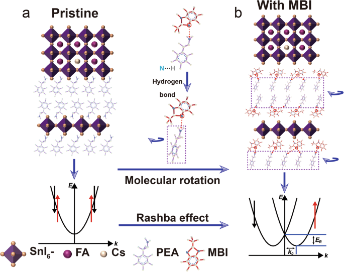
a Schematic diagram of the structure and energy level in pristine Sn-based perovskite semiconductor. b Schematic diagram of the structure and energy level in perovskite ferroelectric semiconductor after doping with MBI molecule.
At the same time, the centers of positive and negative charges do not coincide, leading to the disappearance of central inversion symmetry and the splitting of the energy band. The energy band splitting in ferroelectric semiconductors induces ferroelectricity by resulting in two spin-polarization bands, known as the Rashba effect25. This method of generating ferroelectricity is validated through density functional theory (DFT) calculations, which offer a robust certification for predicting and confirming ferroelectricity26,27,28. This effect will be experimentally verified in the next section.
We further studied material physics using X-ray photoelectron spectroscopy (XPS). Compared to the pristine film, the N 1s peak of perovskite film doped with 0.5 mol% MBI molecule shifts toward lower binding energies, indicating the presence of intermolecular interactions. Specifically, the highly negatively charged N atom in MBI interacts with the N-H group in PEA, resulting in a C-N=C binding energy offset exceeding 0.9 eV. Moreover, the N-H content increased from 8.76 to 35.91% (Fig. 4a, b), providing strong evidence that the source of the ferroelectricity is the MBI molecule-induced hydrogen-bonding reconfiguration. Moreover, the XPS results from other Sn-based perovskite films with different MBI concentrations also show a notable increase in the N-H ratio, compared to the pristine films (Supplementary Fig. 9).
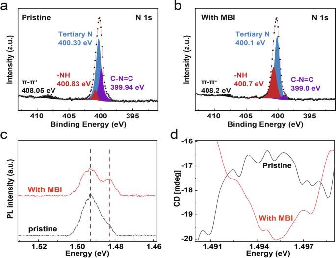
a, b are the X-ray photoelectron spectroscopy of pristine and doped films. c photoluminescence spectra, d circular polarization luminescence spectra.
Photoluminescence spectroscopy (PL) and circular polarization luminescence spectroscopy (CPL) tests were carried out to verify the Rashba effect, which enables their selective excitation by circularly polarized light. With the doping of 0.5 mol% MBI molecule, the PL curve of the perovskite film bifurcates into two peaks, compared to the pristine film. The high-energy peak at 1.493 eV corresponds to the free exciton peak, while the low-energy peak at 1.483 eV is attributed to the indirect transition due to Rashba splitting29 (Fig. 4c). This bifurcation aligns with the disruption of spatial symmetry in the perovskite film, as indicated by the generation of the second harmonic generation (SHG) signal (Fig. 2g). The degree of splitting in the PL peak and the SHG signal varies with the introduction of different MBI concentrations, as illustrated in the Supplementary Fig. 10a, b. The CPL spectroscopy measurements were conducted on both pristine and MBI-doped films to determine the degree of spontaneous energy band splitting. This was achieved by analyzing the disparities in fluorescence spectra excited by left-handed and right-handed circularly polarized light29. Figure 4d demonstrates that MBI doping increased the left-right fluorescence intensity difference at the 1.493 eV emission peak from −16.5 to −20. This enhancement indicates a greater degree of self-selective cleavage, further confirming the Rashba effect.
High-performance transistors based on the ferroelectric perovskite semiconductors
Based on the Sn-based ferroelectric perovskite semiconductor, ferroelectric field-effect transistors (FeFETs) with bottom-gate top-contact structure were fabricated (Fig. 5a). From the transfer curves of pristine transistors, the backward current is lower than the forward current, exhibiting typical interface defects and bulk defects capture carrier characteristics (Fig. 5b). However, due to the effects of polarization-electric field, the backward current exceeds the forward current, indicating pronounced ferroelectric hysteresis for the Sn-based perovskite FeFETs. In addition, the output curves in Supplementary Fig. 11 further suggest that the FeFETs have good contact behaviors, and the contact resistance of the transistor with MBI was measured and determined to be 347 Ω·cm (Supplementary Fig. 12).
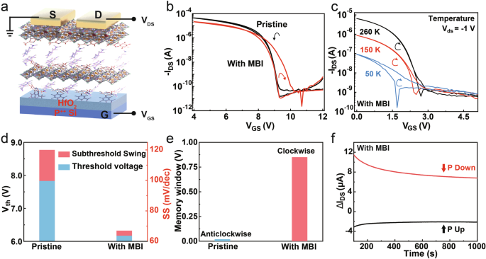
a Schematic diagram of the back-gated transistor structure. b Transfer curves of pristine and doped transistors. c Transfer curves of Sn-based perovskite FeFETs measured at different temperatures. d, e Comparison of the Vth, SS, and memory window values of the pristine and doped transistors. f Memory performance of the Sn-based perovskite FeFETs.
We conducted further measurements of the transfer curves across varying scan speeds, scan ranges, VDS, and temperatures. The scanning window remained largely consistent, reaffirming that the hysteresis originates from the ferroelectricity of FeFETs. More detailed explanations are provided in Supplementary Fig. 13a–e. Moreover, no significant change can be observed in the hysteresis window at varying temperatures within the subthreshold region (Fig. 5c and Supplementary Fig. 13f), thus eliminating the interference from ion migration. From a device-level perspective, the perovskite transistor doped with 0.5 mol% MBI molecule is indeed a FeFET, whose average carrier lifetime of the perovskite layer reaches the highest point compared with other doping ratios (Supplementary Fig. 5). Furthermore, with increasing the MBI concentrations, the hysteresis curves transition from defect-dominated to ferroelectric-dominated, and eventually defect-dominated (Supplementary Fig. 14). Meanwhile, TRPL showed the average carrier lifetime initially rises and subsequently declines, mirroring the trend in film quality (Supplementary Fig. 5). Due to higher doping concentrations, the substantial increase in bulk defects generates a defect field that ultimately overwhelms the ferroelectric field. The predominant bulk defect is a PEA vacancy, which may passivate Sn vacancies30,31,32, allowing for the assessment of PEA incorporation by examining Sn vacancy behavior. XPS results reveal that with increasing MBI incorporation, the concentration of divalent tin vacancies initially rises and then declines (Supplementary Fig. 15). Excessive MBI introduction inhibits PEA incorporation into the two-dimensional structure, leading to the formation of PEA vacancies. The reduction of Sn vacancy reduces the carrier concentration and is conducive to the generation of ferroelectricity.
To further investigate the effects of ferroelectricity, we calculated the key transistor performance parameters, including threshold voltage (Vth) and SS values. After doping with MBI, the Vth decreased from 7.83 to 6.17 V, while the SS decreased from 120 to 67 mV/dec, which extraction method was provided in Supplementary Fig. 1633,34, as given in Fig. 5d, exhibiting the potential for low-voltage operation and low-power consumption devices. Remarkably, the SS value is lower than that observed from two-dimensional α-In2Se3 FeFETs7 (650 mV/dec) and DPPT-TT polymer transistors (85 mV/dec)35, and even approaches the theoretical diffusion limit of 60 mV/dec. This is attributed to the strong ferroelectric field after MBI doping. The polar charge then contributes to gate control and also diminishes the impact of carrier scattering, resulting the high-performance FeFETs11. Compared to the pristine FET, the hysteresis window increases from 0.02 to 0.85 V after MBI doping (Fig. 5e), suggesting an enhanced memory ability. Finally, the memory performance was evaluated by applying 50 write voltages (10 V and 1 s) in opposite directions (Fig. 5f). Both the upward and downward polarization states were sustained for over 1000 s, conclusively proving the memory capability of the ferroelectric transistors.

