Key Takeaways
A new workforce development program jointly led by CNSI, UCLA Samueli and Pasadena City College aims to prepare California students for the growing semiconductor industry. The semiconductor program consists of two phases: a two-week lithography training module and a one-month full-time internship at a designated lab. The federal government enacted the CHIPS and SCIENCE Act of 2022 to invest in U.S. semiconductor manufacturing, research and design and strengthen the supply chain.
A new workforce development program jointly led by UCLA’s California NanoSystems Institute (CNSI), the UCLA Samueli School of Engineering and Pasadena City College aims to prepare California students for the growing semiconductor industry.
Used in countless electronic products, semiconductors power some of the key technologies of the future, including artificial intelligence, quantum computing and advanced wireless networking, which is fueling growth in the industry with giants such as Nvidia Corp., Taiwan Semiconductor Manufacturing Co. Ltd. and Broadcom Inc. quickly becoming household names.
The goal of the Semiconductor Manufacturing Program Pilot is to provide critical hands-on training in the industry and develop a skilled statewide workforce that can support semiconductor companies.
The programs are the final step in a three-pronged approach implemented by CNSI and UCLA Samueli to address California’s workforce development needs. With support from federal and state programs and donors, these programs will increase engagement between students and industry partners and address the need for training aligned with the needs of high-tech employers.
CK Keng Yang, professor and chair of the Department of Electrical and Computer Engineering at the University of California, Los Angeles (UCLA), recognizes the broader importance of this research.
“UCLA is a public university, so our mission is to serve the broader community, not just the students who enroll,” said Yang, lead faculty for the pilot program. “UCLA has a lot of transfer students from community colleges, and they reflect the demographics of California.”
The pipeline is important in addressing weaknesses in the supply chain. For example, when it comes to microelectronics, the US relies heavily on overseas suppliers, especially in Asia. US Commerce Secretary Gina Raimondo has said the US buys 92% of its “cutting edge” chips from Taiwan.
To fill these gaps, the federal government enacted the CHIPS/Science Act of 2022, which aims to invest in American semiconductor manufacturing, research and design, strengthen the supply chain, and invest in America’s future workforce.
“Right now, there is a talent shortage in the U.S. to develop and sustain semiconductor manufacturing,” Yang said. “The industry as a whole will need hundreds of thousands of people over the next few years. We need a lot of talent. Students need expertise in ongoing processes and hands-on experience in the lab to become competent technicians, engineers, and future leaders.”
Yang partnered with Jared Ashcroft, a chemistry professor at Pasadena City College, to create the program.
Aware of CNSI, UCLA Samueli and his involvement with the Department of Defense-funded Microelectronics Commons Southern California site, Ashcroft was eager to create opportunities for students at PCC and other community colleges.
“These programs will give us a fuller picture of training evaluation and research,” said Ashcroft, whose research background is in nanotechnology. “We need not only government support, but industry support as well, and we need data over the long term to show that there’s a return on investment for employers to participate.”
The semiconductor program consists of two phases: a two-week lithography training module and a one-month full-time internship in a designated laboratory. Students receive an allowance to support them during the internship period. The first summer pilot program received 92 applications for 10 spots.
Yang and Ashcroft hope to expand student enrollment and create a program model that can be used for the next cycle and technology. Similar semiconductor training programs are popping up across the United States.
“Our mindset has to change because what doesn’t work in the workforce is competition, and you can’t support students without funding, and you can’t develop programs without funding,” Ashcroft said. “We’re building support systems to provide workers for industry and transfer students for universities.”
Colleges whose students participated in the pilot program included El Camino College, Pasadena City College, Santa Monica College, University of California, Irvine, Moorpark/Ventura College and Mount San Antonio College.
Internship locations include the UCLA Nanofabrication Institute (CNSI and UCLA Samueli), the UCLA High Frequency Electronics Center, the UCLA CNSI Integrated Nanomaterials Institute, and the HRL Laboratory.

Mark Roseboro
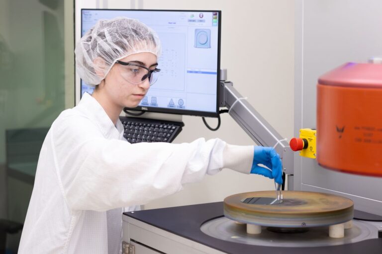
Ani Hakobian of the UCLA NanoLab.
Ani Hakobian, a Pasadena City College student who heard about the program during Ashcroft’s chemistry class, became interested in UCLA’s pilot program as semiconductor manufacturing was on the rise.
Hakobian, a second-year electrical engineering student, hopes to work in the electrical engineering industry after graduation. “This program is very beneficial and gives me valuable experience,” she said.
After her training, Hakobian was assigned to the UCLA NanoLab for her internship. One of the lab assistants happened to be Amber Wang, a friend and high school classmate who was also a UCLA engineering student. For Wang, who helped train Hakobian on the UCLA NanoLab equipment, mentoring her friend was a great plus.
“The opportunities are there,” Wang said. “I tell other students, ‘Put yourself out there.’ Having this educational experience as an undergraduate will be extremely beneficial for my future career.”
For Hakobian, the experience solidified her goal of working in industry: “It gave me a new perspective on the field,” she says. “I’m definitely going to pursue something in chip design and semiconductors.”
The pilot program will continue through next summer, with data tracking being analyzed over the next three to five years to consider students’ continuing education and employment. From Yang and Ashcroft’s perspective, UCLA has a unique opportunity to support the semiconductor industry through this Southern California university ecosystem.

