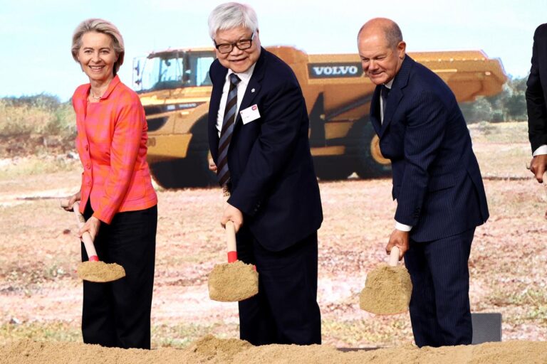
On the left is European Commission President Ursula von der Leyen, and on the right is Chief Executive Officer CC Wey. … (+)
© 2024 BloombergFinance LP
Earlier this week, Europe took a major step forward in its efforts to secure and maintain its technological sovereignty as the European Semiconductor Manufacturing Company (ESMC), a joint venture between TSMC, Robert Bosch GmbH, Infineon Technologies AG and NXP Semiconductors NV, officially broke ground on its first semiconductor fab in Dresden, Germany.
The new large-scale manufacturing facility will produce high-performance chips based on 300mm silicon wafers with node sizes of 28/22 nanometers and 16/12 nanometers using field-effect transistor (FinFET) technology. This advanced process allows the integration of multiple additional functions on one chip, thereby improving performance while simultaneously reducing total power consumption.
The ceremony was attended by prominent figures including European Commission President Ursula von der Leyen and German Chancellor Olaf Scholz, who highlighted the strategic importance of the project.
Von der Leyen announced that the European Commission had approved a German €5 billion measure to support the venture, while TSMC Chairman and CEO CC Wei highlighted the facility’s role in meeting Europe’s growing demand for semiconductors in the automotive and industrial sectors.
The fab is expected to have a monthly production capacity of 40,000 300mm wafers using advanced 28/22nm and 16/12nm process technologies, with a total investment of more than 10 billion euros.
The facility aims to produce 480,000 wafers per year. While not at the cutting edge of semiconductor technology, these nodes are crucial for automotive and industrial applications, and Europe is keen to maintain its leadership in these areas.
Operating as an Open Foundry, a wide range of customers, including European SMEs and start-ups, can place orders and benefit from dedicated support.
As well as technological impact, the project also promises significant economic benefits: ESMC expects to create around 2,000 direct high-tech jobs and additional indirect employment opportunities across the EU supply chain.
And of course, there is also the geopolitical factor to consider: given the uncertainty surrounding political tensions between Taiwan and China, it is important for Europe to reduce its reliance on foreign facilities to avoid being isolated in the event of a conflict.
It is worth noting, however, that in the joint venture to build the Dresden facility, the European partner will only hold a 30% stake, with the rest being held by Taiwan.
Moreover, it is one thing to build a facility based on foreign technology and know-how, but quite another to replicate the same efficiency as in the original environment.
The many challenges facing TSMC’s Arizona chip manufacturing project show that Confucian work ethics, long hours and strict hierarchical systems often do not sit well with Western workers. German trade unions are some of the strongest in the world, so it will be interesting to see how this plays out.
While Europe celebrates this milestone, it must also acknowledge the realities of the global semiconductor industry: the United States has enacted the CHIPS Act, and China is investing heavily in chip technology and making rapid advances.
Currently, the continent’s largest semiconductor project, Intel’s planned €33 billion factory in Magdeburg, is facing delays and uncertainty. With €10 billion in government aid still awaiting approval from Brussels and Intel’s recent financial difficulties, the project’s timeline remains unclear. Construction was scheduled to start in the first half of 2023 but has been pushed back to May 2025 at the earliest.
Whether Europe can implement this ambitious project quickly and effectively will be a key factor in determining Europe’s future role in the global semiconductor industry.
The stakes are high, but so are the rewards.

