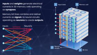
NEO Semiconductor, which focuses on 3D NAND flash memory and 3D DRAM, has unveiled its 3D X-AI chip technology, which replaces the HBM currently used in AI GPU accelerators. This 3D DRAM has AI processing built in, allowing it to process and generate output that does not require mathematical calculations. This reduces the data bus bottleneck issue when large amounts of data are transferred between memory and processors, improving AI performance and efficiency.
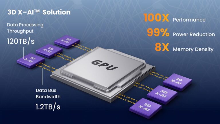
The 3D X-AI chip is based on a layer of neuron circuits that process data stored in 300 memory layers on the same die. NEO Semiconductor says its 3D memory offers 100x performance improvement with 8,000 neuron circuits performing AI processing in memory, eight times the memory density of current HBM, and more importantly, a 99% power reduction by reducing the amount of data that power-hungry GPUs need to process.
“Current AI chips waste a lot of performance and power due to architectural and technology inefficiencies,” said Andy Hsu, founder and CEO of NEO Semiconductor.
Hu commented, “Current AI chip architectures store data in the HBM and perform all calculations on the GPU. In this separated data storage and data processing architecture, the data bus inevitably becomes a performance bottleneck. Transferring large amounts of data over the data bus limits performance and consumes very high power. 3D X-AI can perform AI processing on each HBM chip, which greatly reduces the data transferred between the HBM and the GPU, improving performance and significantly reducing power consumption.”

The company says that X-AI has a capacity of 128GB and can support 10TB/s of AI processing per die, and that stacking 12 dies into a single HBM package can deliver more than 1.5TB of storage capacity and 120TB/s of processing throughput.
AI developments are pushing the boundaries of computing, and many companies are researching techniques to improve processing speeds and communication throughput. As semiconductors become faster and more efficient, the buses that transfer data between components become a bottleneck, so techniques like this allow all components to get faster together.
For example, several companies, including Intel, Kioxia and TSMC, are working on optical technologies to speed up communication within motherboards. But by shifting some of the AI processing from the GPU to the HBM, NEO Semiconductor can reduce the workload and become much more efficient than today’s power-hungry AI accelerators.

